Response to the following problem:
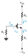
Design the circuit of Fig. for a MOSFET having Vt = 1 V and kn = 4 mA/V2. Let VDD = VSS = 5 V. Design for a dc bias current of 0.5 mA and for the largest possible voltage gain (and thus the largest possible RD) consistent with allowing a 2-V peak-to-peak voltage swing at the drain. Assume that the signal voltage on the source terminal of the FET is zero.