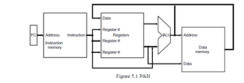
The following diagram reproduces the MIPS Single Cycle Datapath (Figure 5.1) from Computer Organization & Design: The Hardware Software Interface by Patterson and Hennessy.

a) In this representation every instruction takes at most 4 steps to complete a clock cycle. Explain what happens in each step of the clock cycle.
b) Clock cycle time = delay through combinational logic + register setup time + clock skew + delay through register. Briefly explain:
i) Why there is a delay through combinational logic.
ii) What the register setup time is.
iii) What clock skew is.
iv) What the delay through register is.