Question 1:
a) What do you mean by Fermi level? By indicating the position of Fermi level in intrinsic, n-type and p- type semiconductor, describe its significance in semiconductors?
b) Sketch V-I characteristics of a PN diode for the given conditions:
i) Rf = 0, Vγ = 0, Rr = ∞
ii) Rf = 0, Vγ= 0.6V, Rr = ∞
iii) Rf = Non-zero, fixed value, Vγ = 0, Rr = ∞
iv) Rf = Non-zero, fixed value, Vγ = 0. 6V, Rr = ∞
Where Vγ is the cut-in voltage, Rf is the forward dynamic resistance & Rr is the reverse dynamic resistance of the diode.
Question 2:
a) What do you understand about the depletion region at a PN junction, with the help of essential diagrams and derive expression for barrier potential.
b) Derive the expression for transition capacitance, CT of a PN diode.
Question 3:
a) With the help of necessary sketches describe the potential distribution in an open circuited PN junction.
b) With the help of V-I Characteristics, describe the operation of a PN Diode under Forward bias and Reverse bias.
Question 4:
a) Describe Avalanche and Zener break down mechanisms in semiconductors and also compare them?
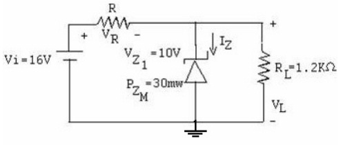
b) For Zener diode circuit shown in figure below, find out VL, VR, IZ & R.

Question 5:
a) Describe the V-I characteristics of Zener diode and distinguish between Avalanche and Zener Break downs.
b) In a Zener diode regulator, the supply voltage = 300V, Vz = 220V, Iz = 15mA and load current = 25mA. Compute the value of resistor required to be connected in series with the Zener diode.
Question 6:
a) Describe the effect of temperature on V-I characteristics of a diode.
b) Differentiate between drift and diffusion current in a semiconductor. Illustrate continuity equation.