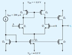
Response to the following problem:
The two-stage CMOS op amp in Fig. is fabricated in a 0.18-μm technology having k1 n = 4k1 p = 400 μA/V2, Vtn -Vtp = 0.4 V.
(a) With A and B grounded, perform a dc design that will result in each of Q1:Q2:Q3:and Q4:conducting a drain current of 100 μA and each of Q6:and Q7:a current of 200 μA. Design so that all transistors operate at 0.2-V overdrive voltages. Specify the W/L ratio required for each MOSFET. Present your results in tabular form. What is the dc voltage at the output (ideally)?
(b) Find the input common-mode range.
(c) Find the allowable range of the output voltage.
(d) With vA = vid/2 and vB =-vid /2, find the voltage gain vo/vid . Assume an Early voltage of 6 V.
