Response to the following problem:
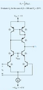
Consider the bias design of the Wilson-loaded cascode differential amplifier shown in Figure.
(a) What is the largest signal voltage possible at the output without Q7: saturating? Assume that the CB junction conducts when the voltage across it exceeds 0.4 V.
(b) What should the dc bias voltage established at the output (by an arrangement not shown) be in order to allow for positive output signal swing of 1.5 V?
(c) What should the value of VBIAS be in order to allow for a negative output signal swing of 1.5 V?
(d) What is the upper limit on the input common-mode voltage vCM?