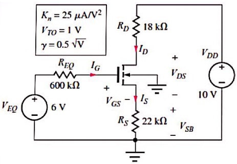
Question 1: Figure depicts a single transistor amplifier; find the biasing point (ID, VDS) of the transistor. Write all required equations to evaluate ID, VDS.
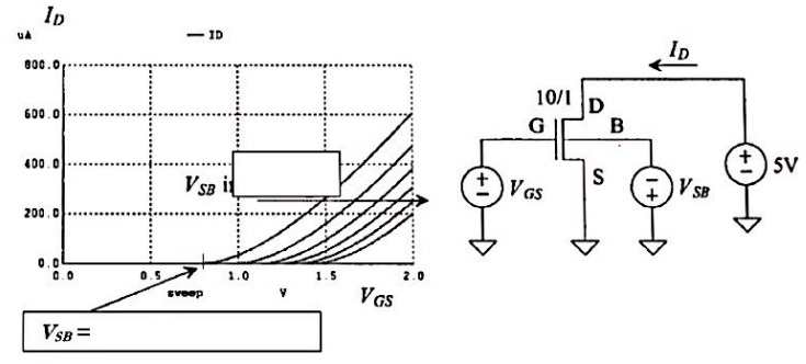
Question 2:
a. Write the equation that describes the body effect on the transistor .
b. On the graph below:
i) Indicate the stating value of VSB on the graph.
ii) Indicate if VSB is decreasing or increasing with the drawn arrow?
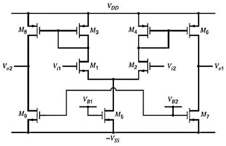
Question 3:
a. What is the topology of the opamp in figure?
b. Is it a fully differential or a single ended opamp?
c. On the figure, determine the +ve and -ve input/output terminals.
d. Redraw the circuit including a common-mode feedback circuit.
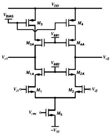
Question 4:
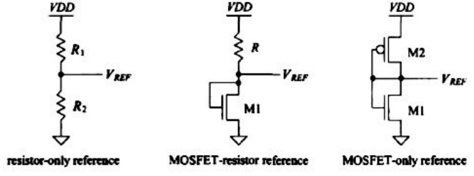
a. Figure (a) shows three voltage dividers circuits. Evaluate VREF for each.
b. In figure (a), which circuit is most suitable for an integrated circuit? Why?
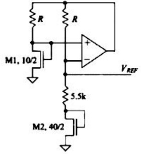
c. Figure (b) depicts a voltage reference circuit. Find VREF
Question 5:
a. Suggest a modification to the circuit to convert it to a single-ended opamp.
b. Which type of current mirror is ised here? State two drawbacks of this type.
c. Redraw the circuit using wilson current mirrors.