Problem 1:
a) Sketch and label the I-V curves of:
i. An ideal diode.
ii. A Germanium diode.
Label the sketched diagrams clearly.
(b) Briefly explains the difference between intrinsic and extrinsic semiconductor.
(c) A circuit is shown in Figure 1. The diodes are germanium type with forward biased voltage of 0.3V.
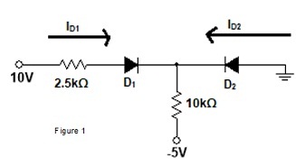
i. Calculate the diode currents ID1 and ID2.
ii. Determine the biasing conditions of diodes D1 and D2.
Problem 2: A silicon bipolar junction transistor (BJT) circuit is shown in Figure 2 required to bias a transistor to half the supply voltage. A transistor model BC107A with hfe of 300 is used and supply voltage, VCC is 12 volts. Given the collector current, IC is 1mA and the base emitter voltage, VBE is 0.7V.
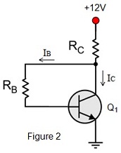
(a) State the name of this circuit configuration.
(b) Explain the advantage of this circuit configuration compared to self-bias circuit.
(c) Explain the mechanism in stabilizing the biasing current of this circuit configuration.
(d) Find the value of RC. Hint: RC = VCC/(2IC).
(e) Find the value of RB. Hint: RB = ((VCC - VBE)*hfe)/(2IC).
Problem 3: The figure below shows an amplifier with current mirror as active load. The MOSFETs have the following parameters: kn' = 300μA/V2, VA(NMOS) = 30V, VA(PMOS) = -15V, Vtn = 26mV, R1 = 5k?, R2 = 12k?, R3 = 400?, L = 0.5μm and W = 5μm. The forward voltage drop in VD1 is 0.7V. Assume the base current of Q4 is negligible compared to emitter and collector currents of Q4 with all the transistors biased in the active region.
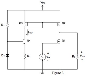
(a) Identify the transistors forming the current mirror.
(b) Calculate the value of reference current, IREF.
(c) Calculate the output resistances of transistors Q1, ro1 and Q2, ro2.
(d) Given that ID1 = kn' (W/L) (VGS1 - Vtn)2, calculate the gate to source voltage of Q1.
Problem 4: Refer to lab manual on Appendix section - Lab Exercise -
Title: BJT DC circuit simulation by using Multisim Live (Drag and Drop).
Objective: To construct and analyze BJT DC circuit by using Multisim Live (Drag and Drop).
Discussions: Write a short report to discuss your answers. Your report should contain a short introduction, some explanation on BJT DC circuit simulation, your experimental procedure, and the results you obtain at every stages of the simulation.
Problem 5: Refer to lab manual on Appendix section - Lab Exercise
Title: Operational Amplifier simulation by using Multisim Live (Drag and Drop).
Objective: To construct and analyze Operational Amplifier circuit by using Multisim Live (Drag and Drop).
Discussions: Write a short report to discuss your answers. Your report should contain a short introduction, some explanation on BJT DC circuit simulation, your experimental procedure, and the results you obtain at every stages of the simulation.
Note - Need in word format and with clear screen shot of for lab answer.
Attachment:- Electrical engineering-lab problems.rar