1. The voltage gain transfer function of an amplifier is:

(a) Write this as a function of:
(i) Radian frequency Av(jω)
(ii) Cyclic frequency Av(jf)
(b) On the sheet of semilogarithmic paper supplied , sketch the (piecewise-linear) Bode plot of the transfer function Av(jf) magnitude in decibels, and phase in degrees both on the same sheet of graph paper and with a common frequency axis (in kHz). Scan that graph and include it with your uploaded submission document.
(c) From your Bode plot, determine the value of the frequency f-180, the frequency at which the phase ∠Av(jf) is -180 degrees. Using your graphs for phase and magnitude, estimate the magnitude (in decibels) at that frequency.
(d) Find algebraically (or iteratively) the actual frequency at which the phase shift ∠Av(jf) = -180 degrees and compare it with your graphical estimate.
2. Refer Sedra & Smith 7th edition, Section E5.1 in Appendix E (or 6th edition Section E6.1, or 5th edition Section D5.1 in Appendix D).
(a) Show the derivation of the expression “tr ≈ 2.2τ” for the 10% to 90% risetime tr of a step response (rising edge of a pulse) passing into a low-pass system with time-constant τ.
(b) Show also the derivation of the expression “tr ≈ 0.35 / f0 ” What bandwidth is needed to pass a 1nsec pulse edge without distortion?
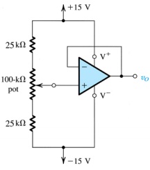
3. Figure (below) shows a circuit that provides an output voltage vO whose value can be varied by turning the wiper of the 100 k? potentiometer.

(i) Find the range over which vO can be varied.
(ii) If the potentiometer is a "20-turn" pre-set device, find the change in vO corresponding to each turn of the pot.
(iii) If the potentiometer is ideal, but the resistors are 1% tolerance and the voltage gain of the op-amp is only 100, what are the maximum and minimum values of vO?
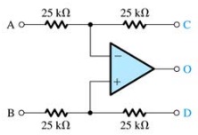
4. Figure (above) shows a representation of a versatile, commercially available lC, the INA105, previously manufactured by Burr-Brown and known as a differential amplifier module. It consists of an op amp and precision, laser-trimmed, metal-film resistors. The circuit can be configured for a variety of applications by the appropriate connection of terminals A, B, C, D, and O.

(a) Show how the circuit can be used to implement a difference amplifier of unity gain.
(b) Show how the circuit can be used to implement single-ended amplifiers with gains:
(i) -1 V/V
(ii) +1 V/V
(iii) +2 V/V
(iv) +1/2 V/V
Avoid leaving a terminal open-circuited, for such a terminal May act as an "antenna," picking up interference and noise through capacitive coupling. Rather, find a convenient node to connect such a terminal in a redundant way. When more than one circuit implementation is possible, comment on the relative merits of each. Taking into account such considerations as dependence on component matching and input resistance.
(c) For a typical instrumentation amplifier, what are the names given to the terminals C and D? Sketch a circuit which shows how the circuit of first Figure can be connected to the circuit of second Figure to provide a unity-gain differential amplifier stage with adjustable output voltage offset.
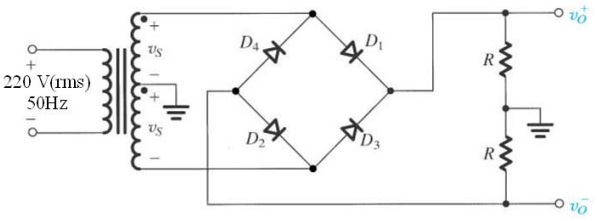
5. Consider the circuit in Figure (below), with two equal-valued filter capacitors placed across the load resistors R. Assume that the diodes available exhibit a 0.7 V drop when conducting. Design the circuit to provide ±l2 V DC output voltages with a peak-to-peak ripple no greater than 1V. Each supply should be capable of providing 100mA dc current to its load resistor R. Completely specify the capacitors, diodes and the transformer.

As well as being widely used in lighting these days, light-emitting diodes (LEDs) are of course used as indicator lights on equipment. A junior student (Fred) decides to use different coloured LEDs, each running at 20mA, to monitor the voltages at various points in the circuit and asks a technician (Carrie) to help to determine the specifications of appropriate “series-dropping” resistors. For the forward voltages, he has obtained the following values from a local hobby store - Red: 2 Volts; Orange: 2.1 Volts; Yellow: 2.2 Volts; Green: 2.3 Volts; Blue: 2.5 Volts.
Fred wants a red LED for the + l2V DC output, blue for the – l2V DC output, orange and yellow for the upper and lower transformer secondary windings. He also wants one (a green one) for the primary (input) winding, which Carrie advises him is potentially hazardous, but she agrees to explain it as a paper exercise providing Fred doesn’t actually do it.
Carrie tells Fred that LEDs tolerate very low reverse voltages (maybe around 5V), so for indication of a.c. voltage, she suggests using two LEDs together (anode of each connected to cathode of the other) such that the maximum reverse voltage applied to each one is limited to the forward voltage of the other.
Determine the “series-dropping” resistors for each LED and sketch them all in place on the final schematic. Indicate what power each of these series dropping resistors will need to be able to dissipate.