Response to the following problem:
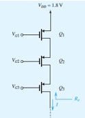
Design the double-cascode current source shown in Fig. to provide I =0.2 mA and the largest possible signal swing at the output; that is, design for the minimum allowable voltage across each transistor.
The 0.13-μm CMOS fabrication process available has Vtp =-0.4 V, V1A =-6 V/μm, and μpCox = 100 μA/V2. Use devices with L = 0.4 μm, and operate at /VOV / = 0.2 V. Specify VG1, VG2, VG3, and the W/L ratios of the transistors. What is the value of Ro achieved?