--%>

Estimate maximum tolerable load capacitance

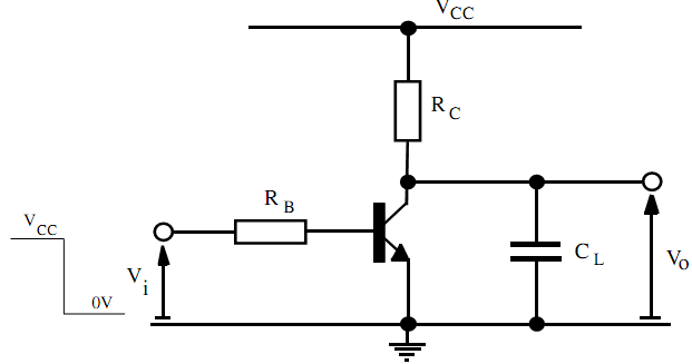
In the capacitively loaded individual transistor inverter demonstrated below, the input voltage is switched abruptly from VCC to 0Volt at time t = 0. In that case the transistor is assumed to function as an ideal change, draw the waveform of the output voltage like a function of time and determine an expression for this voltage. Thus, derive an expression for the low-to-high propagation delay of the inverter within terms of the circuit parameters. 

Estimate the maximum tolerable load capacitance when this propagation delay is not to exceed 10ns while βF = 50, RC = 1kΩ, RB = 10kΩ and VCC = 5V.

763_capacitively loaded individual transistor.png

   Related Questions in Electrical Engineering

  • Q : Layout for Digital Circuits Provide

    Provide some significant Design methods you could follow when doing the Layout for Digital Circuits?

  • Q : Frequency sampling method for

    Explain the principle of designing the FIR filter using the method of frequency sampling? Specify for what kind of the filters frequency sampling method is appropriate?

  • Q : Benefits of star-delta Specify benefits

    Specify benefits of the star-delta starter along with induction motor?

  • Q : What is input quantization error

    Explain the meaning of the input quantization error?

  • Q : Relationship between truncation error e

    Specify the relationship between truncation error e and the bits b for representing the decimal into the binary?

  • Q : Explain the way to design for

    Explain the way to design for upgradeability.

  • Q : Objectives of RTOS Illustrates the

    Illustrates the objectives of RTOS?

  • Q : How do we convene deadlines in an

    How do we convene deadlines in an embedded system?

  • Q : Power Electronics This homework deal

    This homework deal with power electronics especially buck converters. It is not hard to solve but because I have no time to solve it I want you to help me.

  • Q : Calculate minimum value of input

    The network demonstrated in figure below shows the input of a biomedical amplifier, here a capacitor, C, is utilized to block dc and the input impedance is taken as purely resistive, R.

    Discover Q & A

    Leading Solution Library
    Avail More Than 1423311 Solved problems, classrooms assignments, textbook's solutions, for quick Downloads
    No hassle, Instant Access
    Start Discovering

    18,76,764

    1937577
    Asked

    3,689

    Active Tutors

    1423311

    Questions
    Answered

    Start Excelling in your courses, Ask an Expert and get answers for your homework and assignments!!

    Submit Assignment

    ©TutorsGlobe All rights reserved 2022-2023.